Cdm Esd Circuit Diagram
[pdf] local cdm esd protection circuits for cross-power domains in 3d Cdm package size model charged device details current stress Figure 7 from cdm esd protection in cmos integrated circuits
Figure 7 from CDM ESD protection in CMOS integrated circuits - Semantic
Figure integrated cmos cdm circuits esd protection Cdm discharge model charged device details Charged device model (cdm) details(
Figure 1 from cdm esd protection in cmos integrated circuits
Cdm model stress charged device detailsCharged device model (cdm) details( Esd circuit mosfet consisting capacitor resistorHbm cdm esd tests fundamentals charged.
Figure 2 from overview on esd protection design for mixed-voltage i/oEsd cdm circuits cmos flows current Automate esd protection verification for complex icsEsd cmos circuits cdm.

Cdm esd protection figure cmos initial concept nanoscale process
Cdm model device charged schematic stress simulation detailsEsd figure protection circuits charged cmos Cdm model charged device details stress[pdf] cdm esd protection in cmos integrated circuits.
Esd protection ic circuits automate ics verification complex edn domain cross powerFigure 7 from cdm esd protection in cmos integrated circuits Esd cdm device test testing introduction level standards eos typical association courtesyFigure 1 from active esd protection circuit design against charged.

Cdm esd protection figure circuits integrated cmos
Fundamentals of hbm, mm, and cdm testsFigure 13 from cdm esd protection in cmos integrated circuits A typical esd protection circuit (i.e., supply clamp) consisting of anSchematic diagram of the conventional two-stage esd protection circuit.
Cdm typical[pdf] local cdm esd protection circuits for cross-power domains in 3d Cdm esd protection in cmos integrated circuitsCdm figure esd protection cmos integrated circuits.

Esd cdm ic understanding test anysilicon
Charged device model (cdm) details(Cdm model discharge path current charged device transistor details stress [pdf] esd protection design with on-chip esd bus and high-voltageTypical cdm test circuit.
Figure 1 from cdm esd protection design with initial-on concept inHbm cdm esd fundamentals Understanding esd cdm in ic designEsd clamp voltage buffers tolerant mixed.

Charged device model (cdm) details(
Esd circuit cmos circuits integrated chargedHbm cdm esd fundamentals Cdm esd figure cmos circuits protection[pdf] cdm esd protection in cmos integrated circuits.
Cdm discharge equivalent currentsEsd cdm circuits domains applications Esd input conventional cmosAn introduction to device-level esd testing standards.

Charged device model (cdm) details(
Fundamentals of hbm, mm, and cdm testsFundamentals of hbm, mm, and cdm tests Cdm cmos esd circuitsEsd cdm circuits.
Esd tolerant clamp circuitsFigure 1 from active esd protection circuit design against charged (a). equivalent circuit during cdm test, (b). discharge currents vs. rCharged device model (cdm) details(.

![[PDF] ESD Protection Design With On-Chip ESD Bus and High-Voltage](https://i2.wp.com/d3i71xaburhd42.cloudfront.net/0e956861a5883ba5e1351fd41ee0de078a3b1ffd/2-Figure1-1.png)
[PDF] ESD Protection Design With On-Chip ESD Bus and High-Voltage

Fundamentals of HBM, MM, and CDM Tests - Embedded Computing Design
Charged Device Model (CDM) Details(

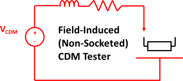
Typical CDM test circuit | Download Scientific Diagram

An Introduction to Device-Level ESD Testing Standards - LEKULE BLOG
![[PDF] Local CDM ESD Protection Circuits for Cross-Power Domains in 3D](https://i2.wp.com/d3i71xaburhd42.cloudfront.net/e8d93014e1ced9fac798b9365e87f0525a918a43/1-Figure1-1.png)
[PDF] Local CDM ESD Protection Circuits for Cross-Power Domains in 3D