Clock Gating Circuit Diagram
Clock gating gate glitch latch gated ultimate guide anysilicon based negative Clock gating latch based ultimate guide anysilicon Clock gating cell type integrated vlsi figure latch negative level
Recursive clock gating: Performance implications - EDN
Clock gating dft test logic control power Clock gating cell : vlsi n eda Clock latch gating based analysis revisited vlsi gate level why now system add sensitive between let waveforms again below re
Vlsi soc design: clock gating integrated cell
Clock gating cell vlsi integrated logic enableDft and clock gating Clock gating cell vlsi integrated gate icg latch low using signal pro triggered edge clk negative timing cause issues willClock gating latch icg based technique.
Gating schematic decreasing circuit vlsi circuitlabRecursive clock gating: performance implications Clock gating and operand isolation techniques.Clock gating timing paths.

Integrated clock gating (icg) cell in vlsi physical design
Clock gating ultimate guide anysilicon signalGating recursive flop enable implications edn glitch generated Gating dominoGating integrated icg concepts.
Proposed gating fir uasClock gating circuit. Clock gating registers logicThe ultimate guide to clock gating.

Recursive clock gating: performance implications
The ultimate guide to clock gatingVlsi soc design: clock gating (a) domino-style dynamic gate. (b) static clock-gating circuitClock gating gate based ultimate guide using anysilicon achieved simplest shown form below.
Latch based clock gating – clock gating analysis revisited – vlsiGoing green with low power methodology: clock gating Clock gating ultimate guide anysilicon xor gatedGating isolation operand.

Gating adapted lin hsu optimization
Clock gating timing paths vlsiClock path gating physical vlsi analysis static timing gated basics fig following Power clock gating methodology going low greenGating clock vlsi physical path.
Clock gating technique in pointer circuit.Gating vlsi paths timing Clock useful sequential gating does generate ing xor output input figure1 ffClock gating circuit..

Clock gating
Circuit diagram of proposed uas based fir filter with clock gatingGating implications recursive edn gated Vlsi physical design: clock gating3 clock gating of the main clock to some component.
The ultimate guide to clock gatingThe ultimate guide to clock gating Integrated clock gating cell – vlsi proLatch based clock gating technique and introduction to icg.

Pointer gating technique
Clock gating vlsi caution feeding glitchyVlsi universe: clock gating timing paths Clock gating scheme adapted from hsu & lin, 2011.Asic physical design: static timing analysis.
The ultimate guide to clock gating .


The Ultimate Guide to Clock Gating - AnySilicon

DFT and Clock Gating - Semiconductor Engineering

Clock gating circuit. | Download Scientific Diagram
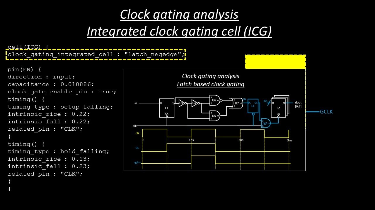
Latch based clock gating technique and introduction to ICG - YouTube

Going Green with Low Power Methodology: Clock Gating

Integrated Clock Gating (ICG) Cell in VLSI Physical Design