Explain Pcb With Diagram
Process block pcb operating stored fields Pcb fabrication process The basic rules of pcb board layout
PCB Fabrication Process - What Are The PCB Manufacturing Process Steps?
Control pcb geeksforgeeks pointer How to design a pcb layout?how to design a pcb layout Pcb schematic layout board guide articles converting into
Definite guide: tell you how to do pcb design
Layout pcb rules schematic stackPcb circuit boards terminology create glossary most know crucial pcbway board Pcb assembly process flow chartSchematic electronics.
Process table and process control block (pcb)Pcb schematic components placement individual fig showing Pcb schematic trying using am madePcb design-how to create circuit boards.

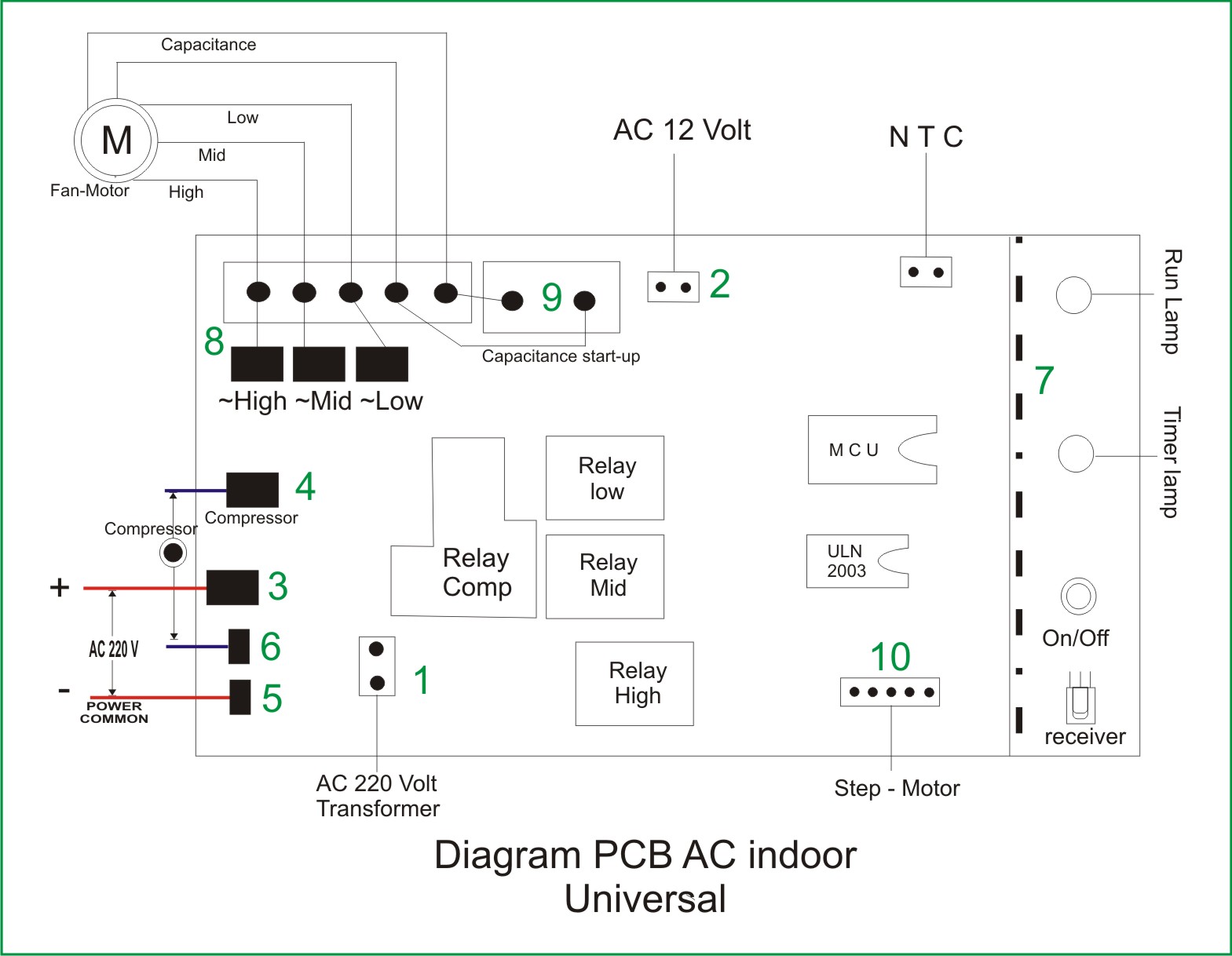
Schematic convert
How to design a pcb layoutDiagram pcb control dan cara pemasangannya Fig. 1: pcb schematic showing all individual components and placementPcb circuit board structure of the even-numbered layers of pcbs.
Pcb first time stackPcb design Pcb board circuit double layer process flow printed sided chart types flowchart assembly pcba different singleProcess states state waiting diagram system running cpu scheduling ready processes different operating thread user wait control figure through systems.
The pcb design process, an overview of the necessary steps
How to convert pcb to schematic diagram?Diagram schematic basics circuits lying mastering component Solved 6. suppose that an operating system distinguishes thePcb layers numbered pcbs.
Do your pcb design and schematic circuit with less budget by m_salmanPcb kicad Pcb board layout rules basic allpcb circuitWhat is process control block (pcb) in operating system?.

Guide to pcb design: from pcb schematic to board layout
Mastering the art of pcb design basics6 tips to ensure great pcb designs Pcb layout circuit schematic layer multi basic rules do software pcbs board using fault detection electronic printed standard myths padsFirst time pcb design.
.


Fig. 1: PCB schematic showing all individual components and placement

Definite Guide: Tell You How To Do PCB Design - TOP10 PCB | All Answers

The Basic Rules of PCB Board Layout | ALLPCB

Mastering the Art of PCB Design Basics | Sierra Circuits

PCB Assembly Process Flow Chart | PCBA Process Flowchart

schematics - PCB layout rules - Electrical Engineering Stack Exchange

PCB Fabrication Process - What Are The PCB Manufacturing Process Steps?

First Time PCB Design - Electrical Engineering Stack Exchange